NJM2374AはPWM制御方式のDC-DCコンバータICで、昇圧・降圧・昇降圧コンバータを実現できます。
新日本無線 | NJM2374A
NJM2374Aのブロック図は下図のようになります。(新日本無線のデータシートより抜粋)

ブロック図を見ただけでは何も分からないので、小ブロックに分割して考えます。
ERR_AMP
内部基準電圧とフィードバックされた出力電圧(IN+端子)を比較・増幅します。データシートにもこのエラーアンプの増幅率は示されていませんが、公開されているspiceモデルを見ると、100倍に増幅しているようです。OSC部
最も分かりにくいのがこのOSC部です。OSC部に接続されているCT端子はタイミングキャパシタと呼ばれるコンデンサを通じてGNDに接続されています。OSC部はタイミングキャパシタへの充放電を繰り返すようになっています。初めにタイミングキャパシタへの充電を行い、タイミングキャパシタの両端電圧が増加していきます。タイミングキャパシタの電圧がある電圧に達すると今度はタイミングキャパシタの電圧を放電します。タイミングキャパシタの両端電圧がある値になったらまた充電を開始して...と動作を繰り返します。
この動作により三角波が生成されます。この三角波の様子はデータシートのタイミングチャートをみるとよくわかります。下図にNJM2374Aのデータシートより抜粋したものを示します。

最終的にこの矩形パルス波がDC-DCコンバータスイッチングの最大デューティとなります。
PWM_COM
PWM_COMはエラーアンプの出力とタイミングキャパシタの発振波形とで比較処理を行います。エラーアンプの出力電圧が上昇すると、OFF期間が長くなるようになっています。
過電流検出部
Ipk Senseと書かれた部分が過電流検出部となります。Siには所望の過電流検出用抵抗を接続します。この過電流検出抵抗の両端電圧を監視することで過電流を検知します。過電流を検知、すなわち過電流検出抵抗の両端電圧が300mV以上となった場合にはPWMロジックの出力を無効化(スイッチングを行わない)するような動作となります。PWMロジック
OSC部からの信号とPWM_COMP、Ipk Senseからの出力を処理してスイッチング素子を駆動する信号を生成します。実装の方針
今回は完全に中身を再現することは目指さず、機能として同等の動作を実現することを考えます。実装の方針をまとめると下記のようになります。
- アナログ入力はERR_AMP入力のみで使用する
- 過電流検出部は実装しない
- タイミングキャパシタを外付けすることはせず、同等の動作を内部にとりこむ
- 出力はPWMロジックのQ出力まで(出力のトランジスタは外付け)
- デバッグなどに使用するため出力イネーブル機能を付ける
HDLコーディング
今回もこれまでと同様にVerilogを使用しました。top階層
素直に実装していきます。//----------------------------------------------
// NJM2374 dc-dc converter test top
//----------------------------------------------
`define POR_MAX 16'hffff
module top(
input clk48, // input clock (48MHz)
output q, // dc-dc converter switching output
input vin, // dsm input(LVDS input)
output vfb_out, // output
input oe // output enable
);
//---- parameter declaration----------------------------------
// Analog to Digital Converter
parameter CIC_TAP_N = 4; // Number of tap step of CIC filter
parameter BIT_W = 9; // output bit width
parameter MAF_TAP_N = 32; // Number of tap step of Mean Average Filter
parameter MAF_SHIFT_N = 6; // Number of shift of Mean Average Filter
// Error Amplifier
parameter ERRAMP_SHIFT_N = 7; // Error Amplifier shift number
// Triangle Oscillator
parameter TRIOSC_BIT_W = BIT_W+ERRAMP_SHIFT_N; // Triangle Wave Oscillator output bit width (unsigned)
// PWM Comparator
parameter PWMCOMP_BIT_W = BIT_W+ERRAMP_SHIFT_N+1; // PWM Comparator input bit width (signed)
//---- generate clock ----------------------
wire clk50;
//
PLL u_PLL(
.inclk0 (clk48),
.c0 (clk50)
);
//---- generate por reset -------------------
wire res_n; // Internal Reset signal
reg por_n; // should be power-up level = low
reg [15:0] por_count;
//
always @(posedge clk48)
begin
if(por_count != `POR_MAX)
begin
por_n <= 1'b0;
por_count <= por_count + 16'h0001;
end else begin
por_n <= 1'b1;
por_count <= por_count;
end
end
//
assign res_n = por_n;
//---- dsm adc ------------------------------
dsm_adc #(CIC_TAP_NUM, BIT_W, MAF_TAP_NUM, MAF_SHIFT_N) u_dsm_adc(
.clk (clk50), // delta-sigma modulator clock
.res_n (res_n), // reset negative
.adc_in (vin), // ADC input
.dsm_fb (vfb_out), // delta-sigma modulator feedback
.adc_out (pos_in) // ADC output
);
//---- err_amp ------------------------------
wire [BIT_W-1:0] pos_in;
wire [BIT_W-1:0] neg_in;
wire [BIT_W+ERRAMP_SHIFT_N:0] out;
assign neg_in = 9'd30;
err_amp #(BIT_W, BIT_W+ERRAMP_SHIFT_N+1, ERRAMP_SHIFT_N) u_err_amp(
.pos_in (pos_in), // positive input(unsigned)
.neg_in (neg_in), // negative input(unsigned)
.out (out) // output
);
//---- triangle wave oscillator ---------------
wire [TRIOSC_BIT_W:0] tri_oscout;
tri_osc #(TRIOSC_BIT_W, 16'd128, 16'd128, 16'd2048) u_tri_osc(
.clk50 (clk50), // clock input(50MHz)
.res_n (res_n), // reset negative
.tri_osc_out (tri_oscout), // oscillator output
.osc_out (oscout)
);
//---- pwm comparator ------------------------
wire comp_out;
pwm_comp #(PWMCOMP_BIT_W) u_pwm_comp(
.pos_in ({1'b0,tri_oscout}), // positive input = triangle wave oscillator output
.neg_in (out), // negative output = error amp output
.comp_out (comp_out)
);
//---- pwm logic ------------------------------
wire pwm_out;
pwm_logic u_pwm_logic(
.tri_osc (oscout), // triangle wave oscillator output
.pwm_comp (comp_out), // pwm comp output
.logic_out (pwm_out) // pwm logic output
);
//---- output enable --------------------------
assign q = ~(pwm_out & oe);
endmodule
assign neg_in = 9'd30;
と指定している箇所が基準電圧入力に対応しています。この値を変えることでフィードバック電圧をどの電圧で制御するのかを決定します。今回は適当に調整して値を決定しています。
今回の実装ではCQ出版のmax10ボードを使用しています。このボードには48MHzの発振器が搭載されていますので、このクロック入力をPLLに入れて50MHzを出力する設定にしています。
ΔΣ型ADC部
基本的には以前実装したとおりです。CICフィルタの中身などは前回のエントリを参照してください。
//------------------------------------------------------------
// Delta-Sigma ADC
//------------------------------------------------------------
//
module dsm_adc(
 clk,   // delta-sigma modulator clock
 res_n,   // reset negative
 adc_in,   // ADC input
 dsm_fb,   // delta-sigma modulator feedback
 adc_out   // ADC output
);

//---- parameter declaration----------------------------------
parameter CIC_TAP_N = 4; // Number of tap step of CIC filter
parameter BIT_W = 9;  // output bit width
parameter MAF_TAP_N = 64; // Number of tap step of Mean Average Filter
parameter MAF_SHIFT_N = 6; // Number of shift of Mean Average Filter

//---- module IO declaration ---------------------------------
input clk;
input res_n;
input adc_in;
output dsm_fb;
output [BIT_W-1:0] adc_out;


//---- Input DFF ---------------------------------------------
//DFF
reg ovs_ff;

always @(posedge clk, negedge res_n)
begin
 if(~res_n)
  ovs_ff <= 1'b0;
 else
  ovs_ff <= adc_in;
end

assign dsm_fb = ovs_ff;

//---- CIC filter --------------------------------------------
wire [BIT_W-1:0] filter1_out;
wire clk_out;

cic_filter #(CIC_TAP_N, BIT_W) filter1(
 .clk (clk),   // clock input (over sampling clock)
 .res_n (res_n),  // reset_n input
 .sig_in (ovs_ff),  // signal input (1bit)
 .sig_out (filter1_out), // signal output (BIT_W bit)
 .clk_out (clk_out) // clock out
);

//---- Moving Average filter ---------------------------------
wire [BIT_W-1:0] filter2_out;

mav_filter #(MAF_TAP_N,BIT_W,MAF_SHIFT_N) filter2(
 .clk (clk_out),
 .res_n (res_n),    // reset_n
 .in_data (filter1_out[BIT_W-1:0]), // input data
 .out_data (filter2_out)
);

assign adc_out = filter2_out;

endmodule
エラーアンプ部
2つの入力の差分をとって適当に左シフト(2の倍数で増幅)します。ちょっとややこしいですが入力は符号なし、出力は符号あり(2の補数表現)としています。
//--------------------------
// Err Amp
//--------------------------
module err_amp(
 pos_in,  // positive input(unsigned)
 neg_in,  // negative input(unsigned)
 out  // output
);

//---- Parameter declaration -----------------------
parameter IN_W = 12;  // input bit width
parameter OUT_W = 19;  // output bit width
parameter BIT_SHIFT = 6; // bit shift

//---- module IO declaration -----------------------
input [IN_W-1:0] pos_in;
input [IN_W-1:0] neg_in;
output [OUT_W-1:0] out;

//---- differential --------------------------------
wire [IN_W:0] diff_signal;

assign diff_signal = {1'b0,pos_in} + ~{1'b0,neg_in} + {{IN_W{1'b0}},1'b1};

//---- bit shift -----------------------------------
assign out = {diff_signal, {BIT_SHIFT{1'b0}}};

endmodule
三角波発振器
ここがおそらく一番ややこしいです。三角波は立ち上がりの時間と立下りの時間が異なっているので注意してください。
ちゃんとNJM2374Aの動作を再現するのであればタイミングキャパシタの両端電圧を確認してそれを再現するべきですが、今回は決め打ちで適当に三角波の振幅を決めています。
また、発振周波数に関しても本来のNJM2374Aよりも高い周波数となるようにしています。
//---------------------------
// triangle wave oscillator
//---------------------------

module tri_osc(
 clk50,  // input clock(50MHz)
 res_n,  // reset negative input
 tri_osc_out, // oscillator triangle wave output
 osc_out  // oscillator output
);

//---- Parameter declaration -----------------------
parameter OUT_W = 18;  // output bit width
parameter CUP_MAX_COUNT = 18'd128;
parameter CUP_RATIO = 18'd256;
parameter CDOWN_RATIO = 18'd4096;

//---- module IO declaration -----------------------
input clk50;
input res_n;
output [OUT_W-1:0] tri_osc_out;
output osc_out;

//---- Oscillator counter --------------------------
reg [OUT_W-1:0] osc_count;
reg countup;    // 0:countup, 1:countdown

always @(posedge clk50, negedge res_n)
begin
 if(!res_n) begin
  osc_count <= {OUT_W{1'b0}};
  countup <= 1'b0;
 end else begin
  if(!countup) begin
   if(osc_count == CUP_MAX_COUNT) begin
    osc_count <= osc_count + ~{{OUT_W-4{1'b0}},4'd8} + {{OUT_W-1{1'b0}},1'b1};
    countup <= 1'b1;
   end else begin
    osc_count <= osc_count + {{OUT_W-1{1'b0}},1'b1};
    countup <= countup;
   end
  end else begin
   if(osc_count == {OUT_W{1'b0}}) begin
    osc_count <= osc_count + {{OUT_W-1{1'b0}},1'b1};
    countup <= 1'b0;
   end else begin
    osc_count <= osc_count + ~{{OUT_W-4{1'b0}},4'd8} + {{OUT_W-1{1'b0}},1'b1};
    countup <= countup;
   end
  end
 end
end

assign tri_osc_out = countup ? (CUP_RATIO * osc_count) : (CUP_RATIO * osc_count);

assign osc_out = ~countup;

endmodule
PWMコンパレータ部
ここは非常にシンプルで2つの入力を大小比較しているだけです。ここだけではないですが、本当であればverilogでは符号付きでレジスタなどを扱えるのでそちらで記述するべきかもしれません。今回は符号付きのものも符号なしで扱っています。比較処理のところでは符号をまず確認するような処理を行っています。
//---------------------------
// PWM comparator
//---------------------------

module pwm_comp(
 pos_in,  // positive input
 neg_in,  // negative input
 comp_out // comparator output
);

//---- Parameter declaration -----------------------
parameter IN_W = 16;  // input bit width

//---- module IO declaration -----------------------
input [IN_W-1:0] pos_in;
input [IN_W-1:0] neg_in;
output comp_out;

//---- comparator ----------------------------------
reg cout;

always @*
begin
 if(pos_in[IN_W-1] & neg_in[IN_W-1]) begin
  if(pos_in[IN_W-2:0] < neg_in[IN_W-2:0]) begin
   cout <= 1'b1;
  end else begin
   cout <= 1'b0;
  end
 end else if(pos_in[IN_W-1]) begin
  cout <= 1'b0;
 end else if(neg_in[IN_W-1]) begin
  cout <= 1'b1;
 end else begin
  if(pos_in[IN_W-2:0] > neg_in[IN_W-2:0]) begin
   cout <= 1'b1;
  end else begin
   cout <= 1'b0;
  end
 end
end

assign comp_out = cout;

endmodule
PWMロジック部
PWMロジックは難しいことは考えず、素直にNJM2374Aのブロック図にある通りに実装します。//--------------------------- // PWM Logic //--------------------------- module pwm_logic( tri_osc, // triangle wave oscillator output pwm_comp, // pwm comp output logic_out // pwm logic output ); //---- Parameter declaration ----------------------- // no prameter //---- module IO declaration ----------------------- input tri_osc; input pwm_comp; output logic_out; //---- pwm logic ----------------------------------- wire andout; assign andout = tri_osc & pwm_comp; wire set_in; wire res_in; assign set_in = andout; assign res_in = ~tri_osc; // rsff wire logic_out_neg; assign logic_out_neg = ~(set_in | logic_out); assign logic_out = ~(res_in | logic_out_neg); endmodule
ピンアサイン
ピンアサインは以下のように設定しました。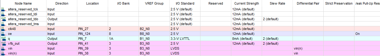
使用リソース
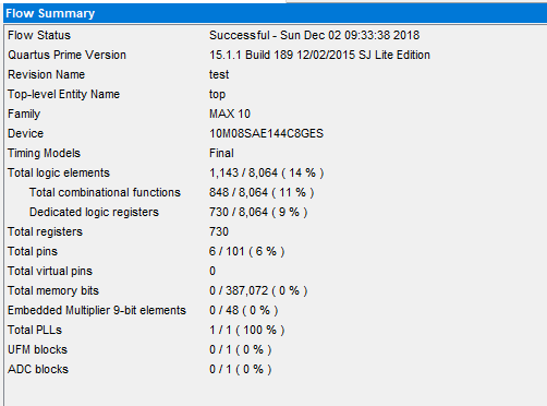
Quartusでコンパイルしたサマリを下図に示します。ロジックエレメント数はおよそ1150程度使用する結果になりました。
動作確認
シミュレーションで動作を確認したら実機で動作させてみます。今回は上記を実装してフライバックコンバータを構成してニキシー管を点灯させてみました。実装はブレッドボードで行っています。
回路図を簡単に書くと下記のようになります。

注意点としては、最終的な出職信号は反転になりますので、反転して出力するようにしています。電源は直流安定化電源から10V程度を出力させています。
最終的にニキシー管点灯電圧の170V付近まで昇圧し点灯させることができました。実際に点灯させるときには電流制限抵抗を入れてください。

ニキシー管はやっぱりきれいですね。
0 件のコメント:
コメントを投稿